Reliability Test Chamber For HBM3 And HBM4 Memory Stacks
HBM stacks memory upward, a dozen thin dies on a base, wired through their middle. The chamber that tests it has to drive heat through the whole height of the tower evenly, slowly enough that the thin silicon does not crack.
HBM gets its speed by going up. It stacks thin DRAM dies one on another, eight or twelve or sixteen high, on a base die at the bottom, then runs thousands of fine copper channels straight down through the silicon to tie every layer together. It is the fastest memory built, the one that feeds the largest processors, packed into a tower under a millimetre tall. That tower is also a hard thing to test. A stack of paper-thin dies, joined by joints smaller than a speck of dust, heats unevenly through its height. A reliability chamber has to bring every layer to the same temperature, gently enough that the thin silicon survives the trip.
What HBM stacks up
The build is a tower of silicon. A finished HBM part is a stack of DRAM dies, each one ground wafer-thin, bonded one on top of the next on a base die at the bottom of the pile. The base die is the controller for the stack, the layer that talks to the processor beside it and routes the traffic down to the board. Above it sit the memory dies themselves, eight in an older part, twelve or sixteen in a current one, with taller stacks already on the way.
The vias are what make the stack one component. A forest of through-silicon vias, fine copper channels punched straight down through each die, carries signal and power from the base up through every layer. Without them the stack would be a pile of separate chips. With them it behaves as a single block of memory, every die reachable through the columns that run its full height.
Between the dies sit the microbumps. Each layer is joined to the one below by an array of solder microbumps, tiny joints that carry the vias’ signals across the gap from die to die. They are smaller than a grain of dust, packed thousands to a die, shrinking with every generation as the stack grows denser. A thin underfill flows around them, gluing the layers together against the stresses ahead.
The whole tower stands under a millimetre tall. A stack of twelve or sixteen dies, with its bumps and underfill, has to fit inside a height near 775 microns, the budget a current HBM part is held to. That ceiling is why the dies are ground so thin, each one a fraction of a normal wafer’s thickness, so a dozen of them and their joints still fit under the height a package allows.
Why building up is its own problem
A flat chip and a stacked one fail in different ways. Lay memory out on a board and each die sits on its own, cooled from above, stressed mainly where it meets the board. Stack the dies and they share everything: one die’s heat passes through its neighbours, one die’s movement pulls on the joints above and below, the dies in the middle sit trapped between the rest. The stack is a system where every layer’s trouble becomes the next layer’s.
The vertical axis is where the new trouble lives. A flat part has little depth to worry about; a stack is mostly depth, a tall thin thing whose problems run top to bottom. Heat has to climb out through the layers. Stress runs up and down the vias. The dies far from the base see a different world from the dies near it. Everything hard about HBM follows from the one choice to build upward.
Thinness compounds the height. To fit the stack under its ceiling, every die is ground to a fraction of its normal strength, so the tower is built of the frailest silicon in the system. A thin die warps more easily and cracks more easily, with less tolerance for a sharp temperature swing. The stack is at once tall and delicate, each of those making it harder to test than the flat memory it replaced.
The vias through the tower
The through-silicon vias are a reliability problem of their own. Each via is a column of copper running down through a die of silicon, two materials that expand at sharply different rates. Copper grows with heat near 16.7 parts per million for each degree; the silicon around it grows near 2.6, the oxide lining it nearer 0.7. Warm the stack and the copper wants to expand far more than the silicon will allow it to.
The copper has nowhere to go but up. Pinned on every side by silicon that holds it tight, a heated via relieves its expansion along the one free axis, pushing its top up above the surface of the die. This is via protrusion, a copper column pumped a little higher each time the stack heats, working against the layer bonded on top of it. Over many thermal cycles the protrusion can crack the dielectric around the via or lift the interface above it.
So the vias set a stress the test has to find. A keep-out zone is left around each via, a margin of silicon kept clear of sensitive transistors, since the stress field of a pumping via reaches into the silicon beside it. The reliability run cycles the stack to drive that pumping, watching for the via that protrudes too far or cracks what it pushes against. The vertical channel that makes the stack fast is also a column of stress running its whole height.
The heat that cannot get out
The hardest thing about a memory tower is that heat struggles to escape it, and the struggle falls unevenly across its height. In a flat chip, heat leaves through the face into a cooler above it, a short trip out. In a stack, the heat made deep in the pile has to travel through every die above it to reach the surface, or down through the base to the package below, a long path crowded with thermal resistance. Each die the heat crosses, each layer of bonding it passes, adds resistance to the escape, so the heat backs up in the middle of the stack where it is hardest to remove. The result is a gradient, the layers near the hot base running well above the layers near the top. Under a heavy workload that gradient can exceed thirty degrees from the bottom of the stack to the top, a thirty-degree difference baked into a part less than a millimetre tall. That gradient is the heart of the HBM reliability problem, because every layer expands by what its own temperature dictates, so a stack with a hot bottom and a cool top is a stack pulling against itself, the warm layers trying to grow while the cool ones hold them back. Each via, each microbump, each bonded interface sits across some part of that gradient, loaded by the difference in expansion between the layer above it and the layer below. Stacking taller makes it worse, because every die added is another sheet of insulation laid over the hot base, trapping more heat in the centre and stretching the gradient wider. A move from twelve dies to sixteen, then toward twenty, piles more thermal resistance onto a heat source that has not shrunk. A reliability chamber cannot treat an HBM stack as a single temperature. It has to drive heat and cold through the whole height of the tower, bringing the buried middle to the same condition as the outer skin, so the stress it measures is the stress the stack would feel in service rather than a gradient the chamber failed to even out. Testing a part that runs hot in its own core, hidden under a dozen layers, is the demand that sets an HBM chamber apart from one built for a flat chip cooled from a single face.
The dies are paper-thin
The dies in the stack are thinner than seems possible. A normal silicon die is hundreds of microns thick, stiff enough to handle on its own. A die in an HBM stack is ground down to a few tens of microns, thinner than a sheet of paper, so a dozen of them fit under the height the package allows. At that thickness silicon stops behaving like a solid block and starts to flex like a film, taking on a warp from stresses a thick die would never feel.
Thinness buys the stack its height, paid for in strength. A die that thin warps under its own stresses, bends when its neighbours bend, cracks where a thicker die would hold. It can carry a tiny flaw from the grinding that a thermal swing later opens into a break. The stack’s speed depends on these wafer-thin layers, so the finished part is only as sound as the frailest sheet inside it.
That fragility shapes how the stack is tested. A thin die cannot take a rough handling or a violent temperature jump the way a thick one shrugs them off; pushed too hard, it cracks where a thick die would only flex. So a reliability run for HBM treads carefully, stressing the stack hard enough to age it without subjecting the thin dies to a shock that a real part would never meet. The test has to be severe on the joints, gentle on the silicon that carries them.
The shape of the problem
A tall stack runs hottest where it is hardest to cool.
The joints stacked layer on layer
Every layer in the stack adds another set of joints to keep sound. The microbumps between two dies carry the signals the vias bring to the gap, so a single cracked bump breaks a connection the same as a cracked via would. A sixteen-high stack has fifteen layers of these joints, each an array of thousands, every one of which has to survive the full life of the part. The count of joints climbs with the count of layers.
The joints shrink as the stacks grow. A microbump that measured twenty or thirty microns in an earlier part is pushed toward ten in HBM4, a smaller pitch packing more connections into the same area. A smaller joint is harder to make without a defect, whether a misaligned pad, a necked solder, or a partial crack, then harder to keep sound under the same thermal stress. The shrink that buys more bandwidth makes each joint a tighter reliability problem.
The industry is reaching past solder for the tightest stacks. Hybrid bonding joins one die to the next with copper pressed straight onto copper, no solder bump between them, closing the gap to nothing. It arrives on the densest future stacks for two reasons. It packs the connections tighter than a bump allows. It also drops the thermal resistance between layers by around a fifth, giving the trapped heat an easier path out. A bonded stack is a different reliability problem from a bumped one, with its own interface to prove.
Where the heat has to go
The heat made in the stack has only two ways out, neither of them easy. It can travel up through the dies to the top of the tower, where a lid or a heat spreader carries it away. It can travel down through the base die into the substrate, then out to whatever cools the package. Both paths cross layer after layer of silicon and bonding, each adding resistance, so neither drains the buried heat quickly.
The path up runs through the memory itself. Heat leaving the hot base has to pass through every die above it to reach the spreader on top, warming each layer as it goes, which is why the dies between the base and the surface run hottest of all. The stacking that gives the bandwidth blocks the heat that the bandwidth makes, a bind with no easy way around it.
Better paths are part of the answer the design reaches for. Bonding the layers copper to copper, with no solder gap between them, cuts the thermal resistance from die to die and gives the heat an easier climb. A thinner bond line and a more conductive joint each shave a little from the gradient, as does a base die built to spread heat as well as to switch it. The cooling of a stack is won layer by layer, the same way the heat is trapped.
Even heat through the height
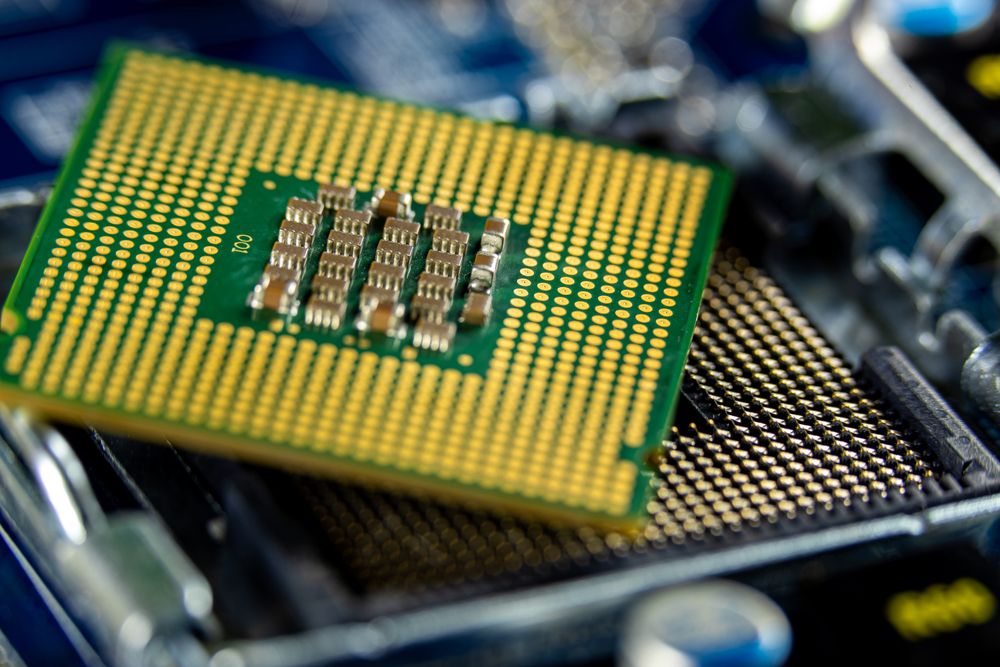
The chamber’s first job is to beat the gradient the stack makes on its own. An HBM part run in a chamber has to reach the test temperature at every layer, the buried middle as much as the outer dies, so the whole tower sits at one condition while it is stressed. A box that heats the surface and leaves the core behind tests a gradient of its own making, layered on top of the one the part already carries.
That asks for heat driven through the depth, not only across a surface. The chamber surrounds the stack with its condition on every face, holding it long enough at each step for the temperature to soak all the way to the centre, so a buried die reaches the same point as a skin die. The thin, resistive path that traps the part’s own heat also slows the chamber’s, so reaching the middle takes a patience the chamber has to allow.
Soak time is the tool for it. Holding the stack at each temperature for long enough lets the heat work through the layers until the gradient inside flattens, so the part is measured at a true uniform condition, never a transient one. A run that rushes from step to step reads a stack still settling, its layers at different temperatures, a result that belongs to the chamber’s haste. The patience to let a tower reach one temperature is what separates a real HBM result from a fast wrong one.
Knowing the inside reached temperature is part of the trick. A sensor on the surface of the stack reads only the skin, leaving the buried middle a guess, so a lab leans on the dwell time and on test structures built into the dies to judge when the core has caught up. The chamber holds each step until the stack’s own readings settle, the sign that the gradient inside has flattened to the condition the test names. A tower brought to temperature on the outside alone is a tower still hiding a gradient within.
Gentle on fragile silicon
Speed of change is the other danger. A thin die cannot take a violent temperature ramp; driven too fast, the thermal shock flexes it harder than it can bear and a fragile layer cracks. The same thinness that lets the stack stand tall makes it intolerant of the sharp swings a sturdier part would shrug off, so the ramp that ages the joints has to stay below the rate that breaks the silicon.
So an HBM profile holds its ramps in check. The temperature climbs and falls at a pace the thin dies can follow, fast enough to stress the joints over many cycles, slow enough that no layer cracks from the speed alone. The test ages the stack the way years of service would, without the single rough shock that would fail a part the field never would. Hard on the joints, soft on the ramp, is the balance an HBM run has to strike.
A stack cannot be reworked
A bonded stack is a one-way build. Once the dies are joined and the underfill is cured, there is no taking a bad layer out, no replacing a cracked die or a failed via deep in the pile. A single bad layer dooms the whole tower, every good die above and below it lost with the one that failed. The value bound into one stack is the sum of all its dies, committed past recall.
That irreversibility raises the stakes of the test. Each die is tested before it joins the stack, so a known-bad layer never gets bonded in. The finished stack is tested hard because a failure found later cannot be repaired, only scrapped. A part this valuable, this impossible to fix, is one the reliability run has to catch in the lab. The chamber guards a build that allows no second chance.
Reaching a fault inside the stack is its own difficulty. No probe can touch a die buried under a dozen others, so the stack is exercised through the base die’s interface, the one door into the whole tower. A failure deep in the pile shows only as an error read out through the bottom, so the test leans on reading the stack electrically as the chamber works it, catching the layer that drops out without ever seeing it directly. A part this sealed gives up its faults only to the instrument patient enough to read them through the base.
Damp and the stack
Moisture finds the polymers in the stack. The underfill between the dies and the films around the joints are organic, so they take up water from damp air the way any plastic does. The water gathers at the bonded interfaces, weakening them, readying a delamination that the next thermal swing can pull open between two layers.
So an HBM chamber damps the stack as well as cycling it. Holding the part at heat and humidity drives moisture into its organic layers, so the test sees a stack carrying the water a humid life would load into it. In a tower where every interface is already loaded by the thermal gradient, a damp-weakened bond is one more way a layer can let go, which the test has to provoke before the field does.
From HBM3 to HBM4 and beyond
Each generation makes the tower harder to hold together. HBM3 gave way to parts that stack higher and run wider, drawing more power through the same small footprint, so the heat to remove and the layers to cross both climb together. HBM4 widens the interface and adds a logic base die built on an advanced process, a hotter, busier floor under the memory above it.
More layers mean a steeper climb for the heat. A move from twelve dies to sixteen, then to twenty in the generations being planned, lays more insulation over the base and widens the gradient the chamber has to flatten. The thickness budget creeps up to make room, toward 825 or 900 microns for the tallest stacks. The dies grow thinner still to fit inside it, trading one fragility for another.
The reliability question only sharpens with each step. A stack that is taller and hotter, bonded more tightly, carries more joints across a wider gradient, every one a place to fail, so the chamber that qualifies it has to push harder, staying gentler than ever on silicon ground thinner than before. The demand on the test rises with every layer the design adds.
What an honest HBM chamber provides

Everything an HBM chamber needs comes back to the tower it tests. The stack runs hot in a buried core and stands on the frailest silicon in the system, failing at any of a thousand joints across its height. A chamber that can stress all of that, honestly, has to do a few things at once that a simpler box never has to.
It has to reach every layer. The chamber brings its temperature to the buried middle of the stack as surely as to the outer skin, holding each step long enough for the heat to soak through the depth, so the part is stressed at one condition, never a gradient. Uniformity through the height, not only across an area, is the first thing an HBM chamber proves.
It has to ramp with care. The temperature changes slowly enough that the thin dies follow without cracking, so the stress comes from the cycling the test intends, never from a shock the ramp imposed. The gentleness is not a soft spot in the test; it is what lets the test reach a fragile part without breaking it the wrong way.
It has to add moisture and hold it steady. The organic layers in the stack need the damp-heat stress that finds their weak bonds, so the chamber controls humidity alongside temperature, across the long soaks a tall stack demands. Holding both steady through a slow, deep run is part of what the box has to deliver.
The measure of it all is whether the result belongs to the stack. An HBM chamber done right brings the whole tower to one true condition, stresses it the way service would, then leaves only the stack’s own response, its protruded via, its fatigued bump, its cracked thin die, with nothing of the chamber’s gradient or haste mixed in. That is the demand a tower of memory places on the box that proves it: reach the buried middle and spare the fragile silicon, then read back only what the stack itself would feel.
Common questions
What is an HBM memory stack?
HBM, high-bandwidth memory, stacks thin DRAM dies one on another, eight to sixteen high, on a base logic die, wired together by copper through-silicon vias that run down the full height. The stack acts as one block of memory, packed into a tower under a millimetre tall, feeding the largest processors. Its speed comes from building memory upward instead of laying it out flat.
Why is an HBM stack hard to test for reliability?
The stack heats unevenly through its height and runs on dies ground to a few tens of microns, then fails at thousands of tiny joints between layers. A chamber has to bring the buried middle to the same temperature as the outer dies, then stress the part without cracking the fragile silicon. The vertical and thermal nature of the tower, built of delicate silicon, makes it harder to test than flat memory.
What is the thermal gradient in an HBM stack?
Heat made deep in the stack struggles to escape through the layers, so it backs up in the middle, leaving the bottom layers hotter than the top. Under a heavy workload the difference can exceed thirty degrees across a part under a millimetre tall. That gradient stresses every via and joint. It is the central problem an HBM reliability test has to reproduce honestly.
What is TSV copper protrusion?
A through-silicon via is a copper column running down through a silicon die. Copper expands with heat far more than silicon, so a heated via, pinned on its sides, pushes its top up above the die surface. Over many thermal cycles this protrusion can crack the dielectric or lift the layer bonded above it, which is one of the failures an HBM reliability run is built to find.
Why must the chamber ramp slowly for HBM?
The dies in the stack are ground paper-thin to fit under the height limit, so they crack under a violent temperature swing a thicker die would survive. A slow ramp lets the thin silicon follow the temperature without a shock, still cycling the joints enough to age them. The run has to stress the joints hard, staying gentle on the fragile dies.
Part of the Envsin guide to semiconductor reliability testing. An HBM chamber drives heat through the whole height of a stacked tower, evenly and slowly, so the stress it measures is the stack’s own, the response that decides whether a tower of thin memory holds together.